Conductor technology of the future: Walter Lemmen showcases innovative devices at electronica 2024
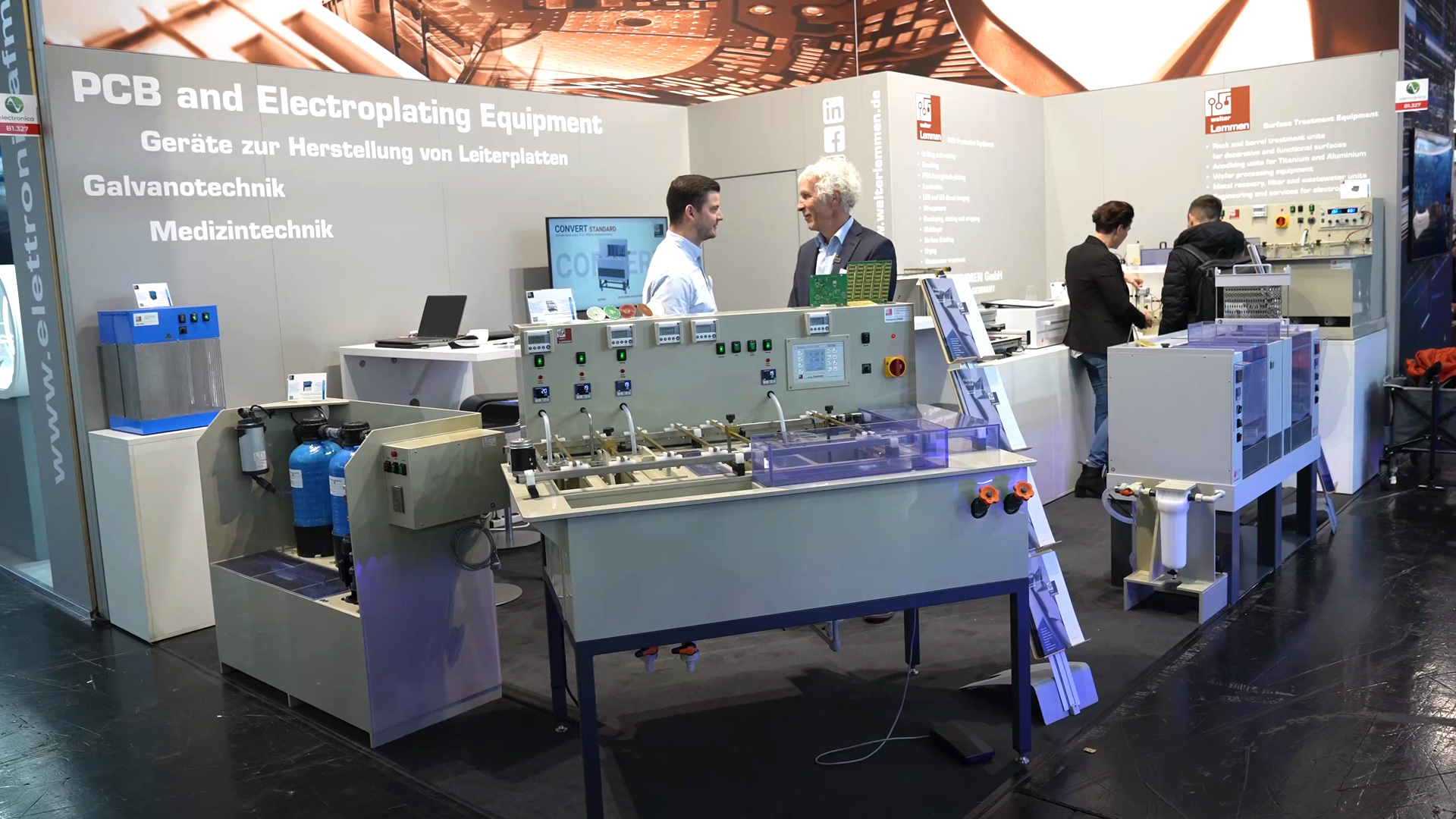
Walter Lemmen GmbH, based in Kreuzwertheim, has been a leading manufacturer of electroplating and PCB technology products for industry, research and education for over 40 years. The company develops and manufactures a wide range of systems in Germany, which are sold worldwide. The product range includes equipment for the production of single or double-sided PCBs through to through-plated PCBs and multilayers for prototype and small series production. Customized small electroplating systems for barrels and racks complete the portfolio and enable the finishing of various materials for decorative and functional surfaces.
Lemmen: Specialist for the production technology of printed circuit boards
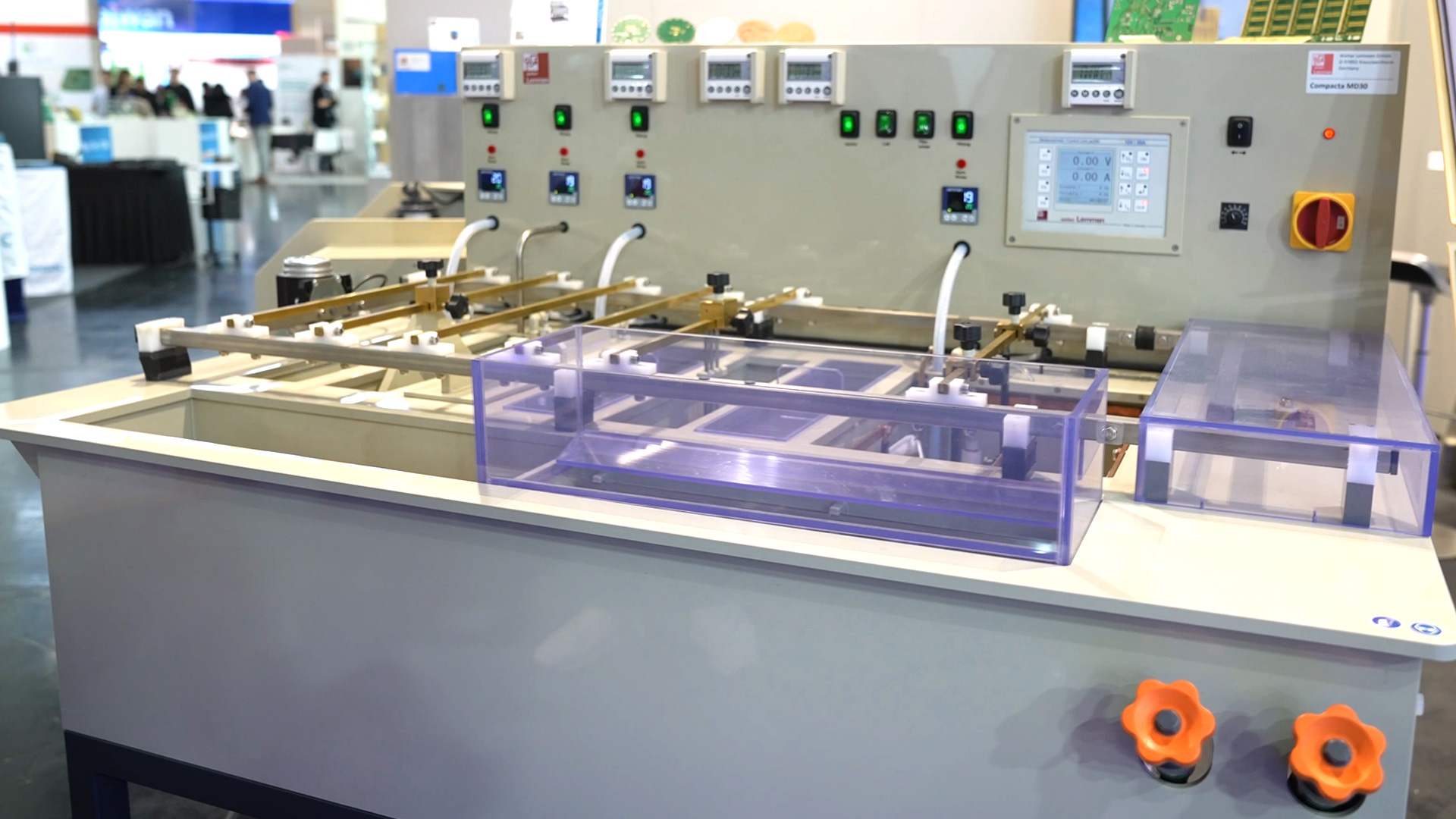
Lemmen offers highly specialized equipment for the production of printed circuit boards and covers all production processes, from mechanical and photochemical to galvanic processes. The systems are particularly suitable for the production of prototypes and small series. At the electronica trade fair, Lemmen is currently presenting its innovative equipment for through-hole plating of printed circuit boards. This process involves drilling the circuit board and then copper-plating the drill holes to create an electrical connection between the layers. Lemmen uses environmentally friendly processes and advanced electroplating technology for these steps.


Customized solutions and applications in electroplating technology
Lemmen develops its systems specifically tailored to customer requirements. Its main clients include renowned research institutes such as the Max Planck Institute, Fraunhofer, DLR and various universities. The systems can be adapted in many ways and can integrate special surface finishing processes such as nickel or gold coatings on request. This flexibility enables research institutes to produce prototypes and small series with individual requirements and to carry out complex production processes directly in the system.

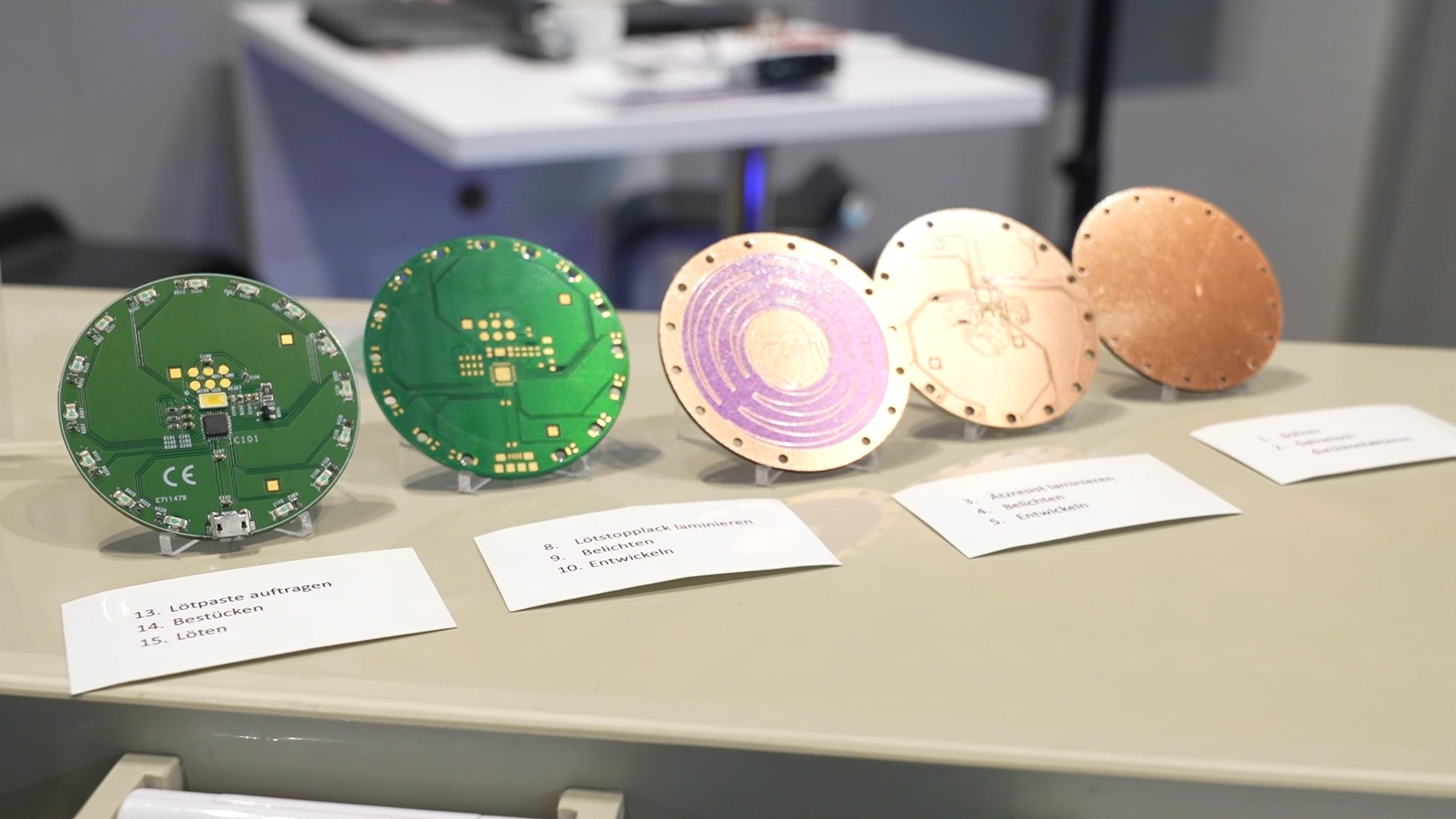
Efficient through-hole plating and multilayer technology for precise PCB production
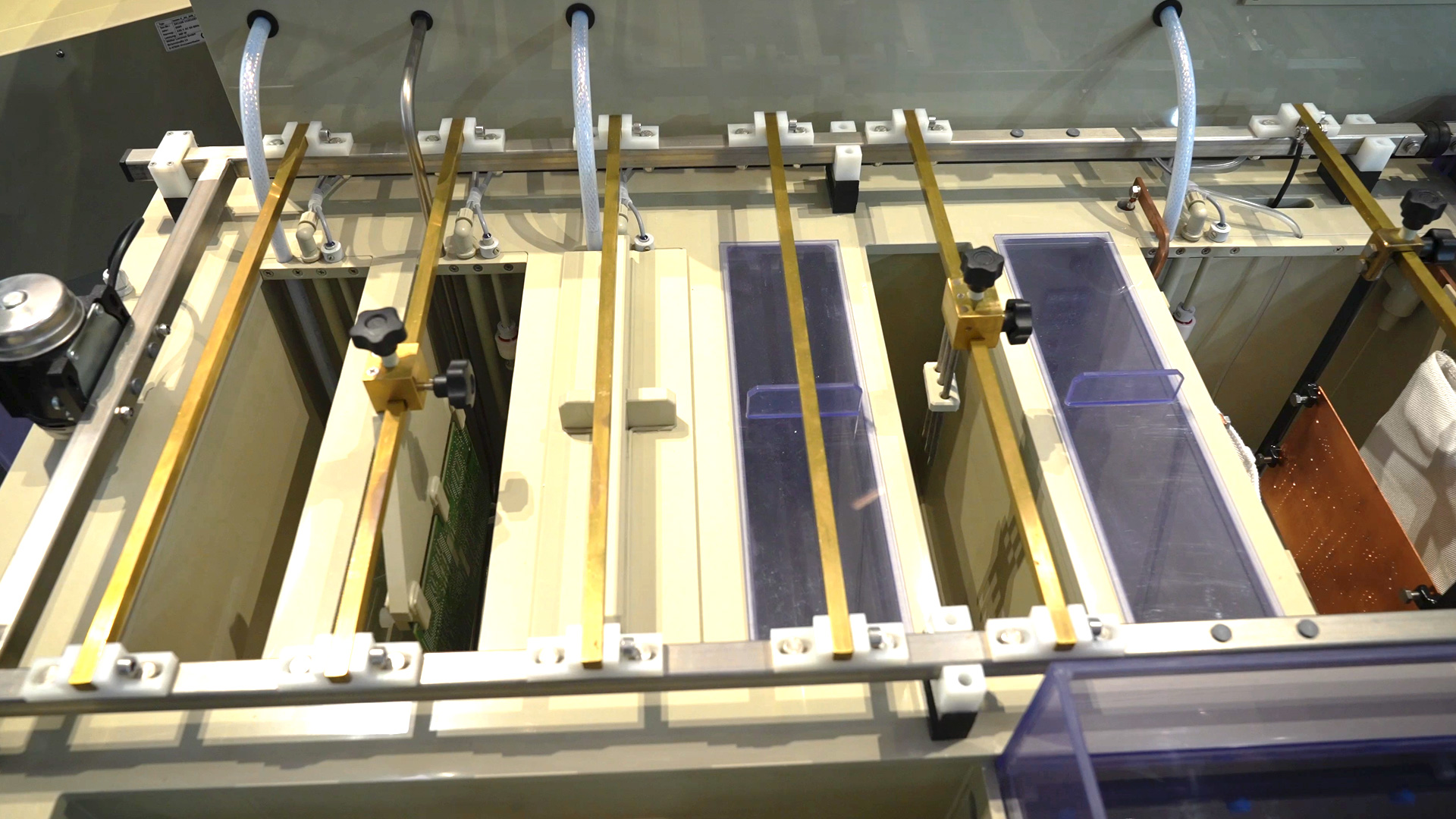
A particular strength of the Lemmen devices is the precision of the through-hole plating process and the ability to produce multilayer PCBs. After through-hole plating, photolayers are applied and exposed and the copper layers are etched. For final protection and improved solderability, the PCB can be coated with a solder paste and then finished with copper, nickel or gold. This detailed production enables the production of printed circuit boards with several layers, which are indispensable for demanding applications in electronics research and development.
