ASMPT AMICRA NANO: High-precision die bonder for photonic applications
by A. Bergmeier - 2024-11-26ASMPT is a leading global provider of hardware and software solutions for the manufacture of semiconductors and electronics. Headquartered in Singapore, the company offers solutions for all key steps in the electronics manufacturing process, from wafer coating, chip assembly and packaging to surface mount technology (SMT). ASMPT's products are used in various end devices such as cell phones, computers, automobiles and LED displays.
AMICRA NANO: Precision and innovation in die bonding for photonic applications
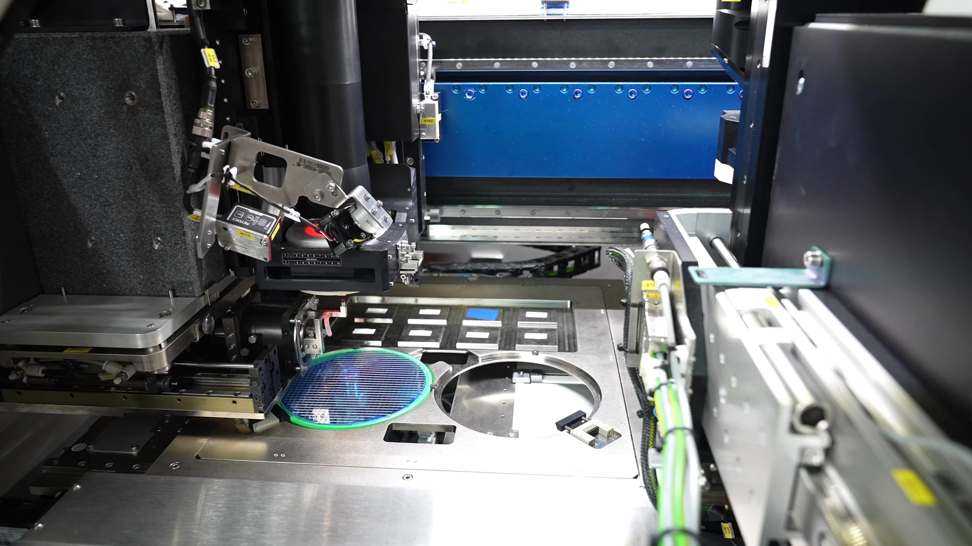
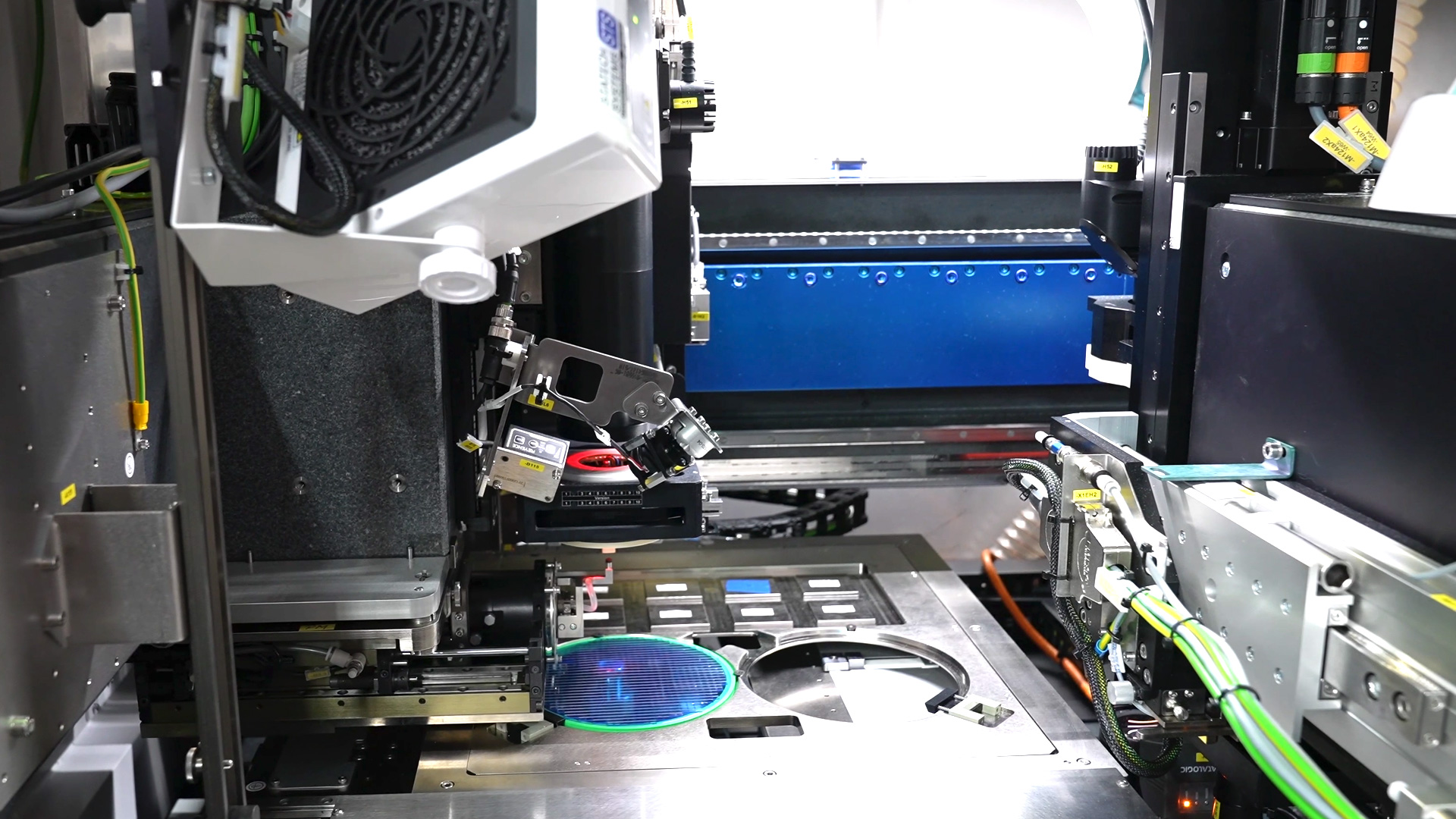
The AMICRA NANO, presented by ASMPT, sets new standards in die bonding technology. With a placement accuracy of 200 nanometers, it is the most precise die bonder on the market and is specially designed for photonic applications. This impressive precision makes it possible to meet the requirements of state-of-the-art technologies where the highest accuracy is crucial.

Unique technologies for maximum precision
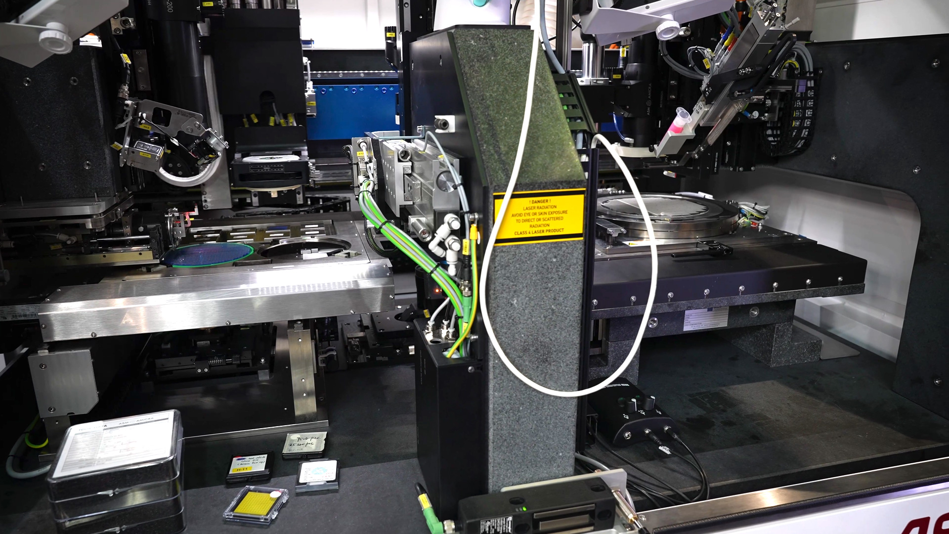
The key to the outstanding performance of the AMICRA NANO lies in the patented Lyman alignment concept. The bonding tool is designed so that a central hole allows a simultaneous view of the die and the substrate. This unique innovation ensures exact alignment and precise bonding. By using advanced image processing technology, every step of the bonding process is monitored and optimized.
Efficient processing for high throughput rates
In addition to its exceptional accuracy, the AMICRA NANO also impresses with its efficiency. Up to 200 dies can be processed per hour, using both gluing and soldering processes. This makes the machine ideal for industrial applications where precision and speed are equally important. The entire process, from die input to final positioning, is designed for maximum efficiency and user-friendliness.

Intelligent user interface for optimum control
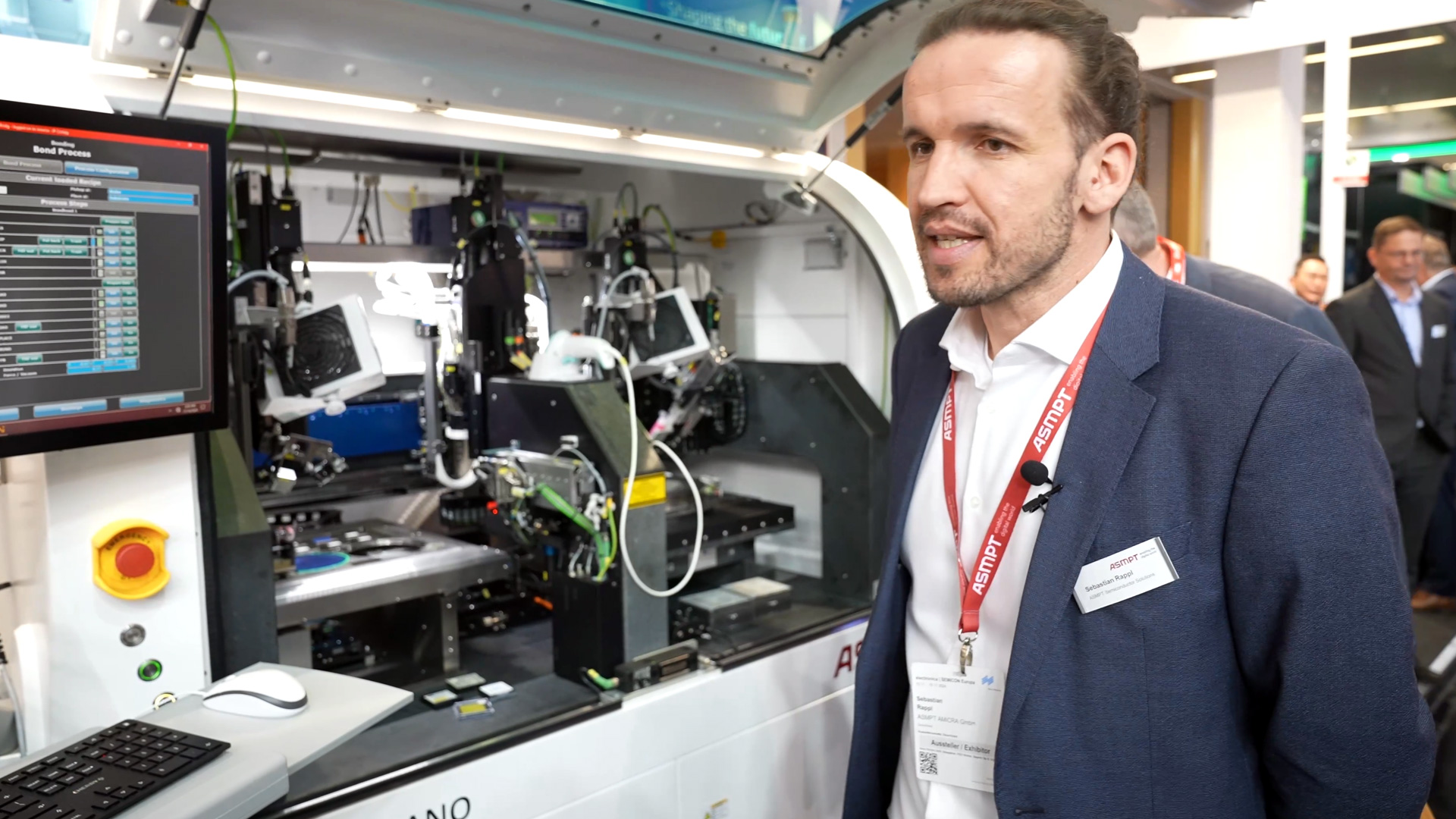
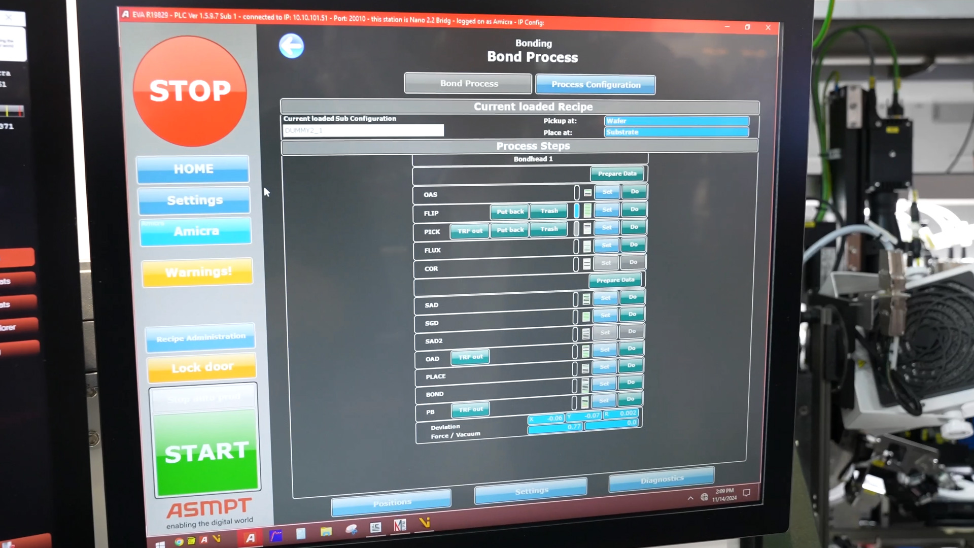
The user interface of the AMICRA NANO offers a clear and intuitive display of all steps of the bonding process. The individual process steps that each die goes through are displayed on the right-hand side, while image processing and alignment are monitored on the left-hand side. This user-friendly interface enables easy operation and ensures optimal results.
